


ADI公司的ADP1614是一款内部集成输出达到20V电压的功率开关的升压型DC/DC转换器,ADP1614采用外部电阻的设置限制输出电流的大小,ADP1614采用两种固定的增压开关频率,分别为650KHz和1.3MHz。ADP1614在对空间有约束的应用中占有很大优势,常用于便携式产品中。ADP1614具有在电流模式下PWM效率达到94%,使能器件可调软开关保护涌入电流,在电流模式下具有优秀的瞬态响应,同时具有欠压闭锁、过热保护等特点。本文通过总结ADP1614器件的特点,介绍器件、特性、应用方向及内部结构框图,并给参考设计实例原理图、制板图及元器件清单。
The ADP1614 is a step-up, dc-to-dc switching converter with an integrated power switch capable of providing an output voltage as high as 20 V. The ADP1614 is available with a pin-adjustable current limit that is set via an external resistor. The boost switching frequency is fixed to either 650 kHz or 1.3 MHz. With a package height of 0.8 mm, the ADP1614 is optimal for space constrained applications, such as portable devices or thin film transistor (TFT) liquid crystal displays (LCDs).
The ADP1614 operates in current-mode pulse-width modulation (PWM) with up to 94% efficiency. Adjustable soft start prevents inrush currents when the part is enabled. The PWM current-mode architecture allows excellent transient response, easy noise filtering, and the use of small, cost-saving external inductors and capacitors. Other key features include undervoltage lockout (UVLO), thermal shutdown (TSD), and logic controlled enable.
The ADP1614 is available in a Pb-free, 10-lead lead frame chip scale package (LFCSP).
ADP1614主要特性:
Adjustable current limit, up to 4 A
2.5 V to 5.5 V input voltage range
650 kHz or 1.3 MHz fixed frequency option
Adjustable output voltage, up to 20 V
Adjustable soft start
Undervoltage lockout
Thermal shutdown
3 mm × 3 mm, 10-lead LFCSP
Supported by ADIsimPower design tool
ADP1614应用:
TFT LCD bias supplies
Portable applications
Industrial/instrumentation equipment
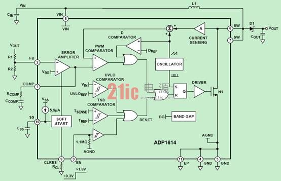
图1. ADP1614方框图
ADP1614参考设计主要特性:
2.5 V to 5.5 V input voltage range
650 kHz or 1.3 MHz fixed frequency options
Adjustable current limit up to 4 A
Output voltage
5 V for ADP1614-650-EVALZ
15 V for ADP1614-1.3-EVALZ
Jumper for enable/shutdown control
Components optimized for the indicated output voltages
ADP1614设计原理图:
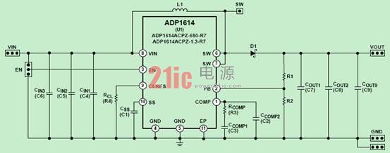
图2. ADP1614设计原理图[!--empirenews.page--]
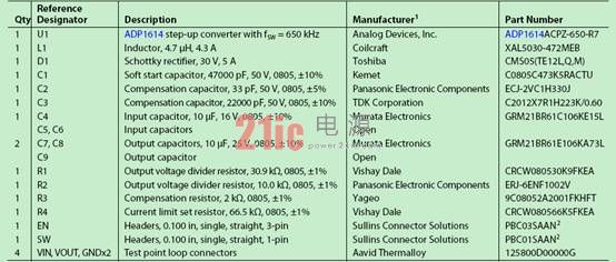
ADP1614 (fSW = 650 kHz, VOUT = 5 V) 设计方案材料清单:
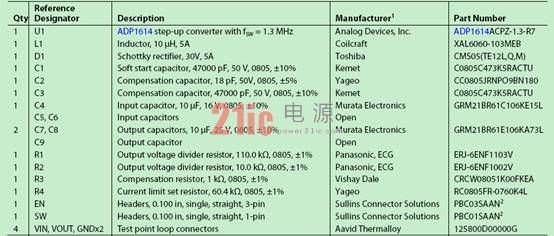
ADP1614 (fSW = 1.3 MHz, VOUT = 15 V) 设计方案材料清单:
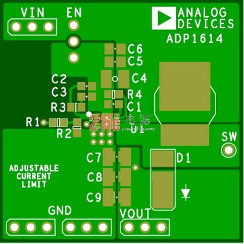
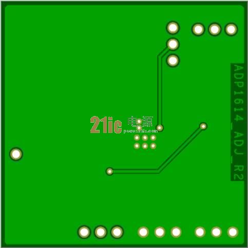
PCB元件布局图: